NVIDIA Vera CPU Accelerates Chip Design — AI Hardware's New Feedback Loop
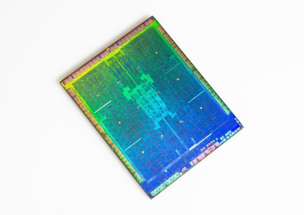
NVIDIA is using its Vera CPU to accelerate next-generation chip design. In collaboration with Cadence and Synopsys, Vera delivers up to 1.5x higher performance on critical simulation and verification workloads.
When a Chip Designs Its Own Successor
The semiconductor industry has always sought ways to accelerate chip design and manufacturing. In July 2026, NVIDIA published a milestone announcement that captured the industry's full attention: the company is using its own Vera CPU to supercharge the EDA (Electronic Design Automation) workloads used to design its next generation of CPUs and GPUs.
This is far more than another benchmark milestone. It represents a fundamental strategic shift — a virtuous flywheel where NVIDIA's CPUs help design better NVIDIA CPUs and GPUs. Early testing already shows up to 1.5x higher performance on critical verification and simulation workloads from industry leaders Cadence and Synopsys.
Vera CPU Architecture: 88 Olympus Cores, Purpose-Built
Vera is not an off-the-shelf server processor. It integrates 88 custom NVIDIA Olympus CPU cores paired with a high-efficiency LPDDR5X memory subsystem and the second-generation NVIDIA Scalable Coherent Fabric. This combination delivers strong per-core performance, high memory bandwidth, and consistently low latency — precisely the characteristics that demanding engineering workloads require.
This architecture is especially well-suited to the dual nature of EDA workloads. Engineers need low-latency execution for individual simulation runs and massive throughput for large-scale regression testing across compute farms. Vera's design optimizes for both, enabling faster verification cycles and allowing engineers to evaluate more design alternatives within the same development window.
Up to 1.5x Performance on Cadence Jasper and Synopsys VCS
NVIDIA's initial testing focused on two of the most compute-intensive stages of modern chip design. Cadence Jasper, a formal verification platform, uses smart proof technology and machine learning to detect and fix bugs early in the design cycle. Synopsys VCS, a high-performance functional verification solution, simulates and validates complex chip designs before fabrication.
Both applications showed up to 1.5x higher performance on selected production-class workloads — and critically, the tests used the same number of cores. This means Vera's advantage does not come from sheer core count but from superior per-core performance, an efficient memory hierarchy, and a low-latency interconnect fabric.
Beyond these benchmark results, NVIDIA is already working closely with Cadence and Synopsys on application profiling, software optimization, and system-level tuning. The goal is to improve engineering productivity across a broader range of EDA workflows over time, extending Vera's impact well beyond the initial benchmarks.
From RTL to Silicon: The EDA Pipeline
Modern chip design begins at the register-transfer level (RTL), where engineers describe a processor's behavior. From there, a complex pipeline of verification, implementation, and testing transforms the design into manufacturable silicon — a process that spans years.
While GPUs and AI have dramatically accelerated many aspects of chip design, logic simulation, formal verification, and portions of digital implementation remain heavily CPU-dependent. These workloads require fast single-thread performance and efficient memory systems, making CPU architecture a critical factor in overall design cycle time.
Vera addresses precisely this bottleneck. By delivering up to 1.5x faster verification runs, it enables engineering teams to validate more designs, catch corner cases earlier, and reduce costly late-stage design iterations.
The Feedback Loop: NVIDIA CPUs Designing NVIDIA Chips
The broader story here goes beyond Vera's specifications. NVIDIA is deploying Vera across the EDA workflows used to create future NVIDIA processors, creating a continuous feedback loop between silicon design, software optimization, and systems engineering.
Vera speeds up the design of the next-generation CPUs and GPUs. Those faster, more capable chips will in turn enable even more sophisticated EDA workloads. And looking ahead, NVIDIA has already announced plans for the next-generation Rosa CPU, powered by the NVIDIA Rigel core, which will continue this virtuous cycle.
Strategic Collaboration With Cadence and Synopsys
NVIDIA's collaboration with Cadence and Synopsys is central to this strategy. The three companies are working together on application profiling, software optimization, and system-level tuning designed to extract maximum performance from Vera's architecture across a wide range of EDA tools.
Looking Ahead: Rosa, Rigel, and the Future of Chip Design
With Vera already deployed in production EDA workflows, NVIDIA is looking ahead to its next-generation CPU platform. Rosa, powered by the new Rigel core, will build on Vera's foundation and extend the performance envelope further.
This approach — using NVIDIA CPUs to design better NVIDIA CPUs and GPUs — represents a paradigm shift in the semiconductor industry. It creates a self-reinforcing cycle of improvement where each generation of silicon helps build a faster, more capable successor.
Conclusion: A New Era for Semiconductor Design
NVIDIA's Vera CPU announcement marks a turning point in how the semiconductor industry thinks about chip design. The 1.5x performance gains on Cadence Jasper and Synopsys VCS are proof that a tightly integrated hardware-software strategy can deliver tangible results.