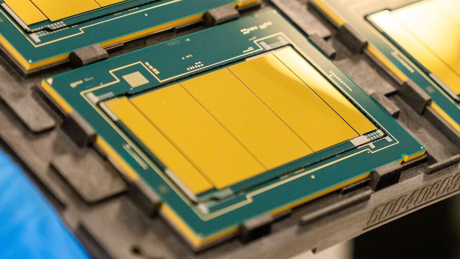
Intel Maps Next Steps for EMIB and Foveros Chip Packaging
Intel outlines how EMIB bridges and Foveros packaging will support larger AI and data center packages, finer bump and hybrid bonding pitches, glass substrates, and stacked modules linked into heterogeneous system in packages.
EMIB moves toward finer bridges and larger packages
Intel says advanced packaging is now integral to high end client and data center CPU designs, with EMIB and Foveros used across many recent multi chiplet products. The company argues that its multi chiplet strategy can deliver performance and feature gains cost effectively and on a predictable cadence, even though not every project has been a success. The stated goal is to build system in packages approaching 12 reticles by combining EMIB with Foveros Direct 3D.
EMIB entered high volume manufacturing in 2017 and still uses small silicon bridges embedded in an organic substrate only where dense die to die links are needed, instead of a large silicon interposer. Intel reduced the first layer interconnect bump pitch from 55 µm to 45 µm, with roadmaps pointing to about 36 µm and later 25 µm. EMIB-M adds metal insulator metal capacitors to improve power delivery, while EMIB-T adds through silicon vias so power can move vertically through the bridge. Intel said EMIB-T is on track for mass production in 2027 and that yields and reliability are meeting targets.
Foveros adds interposer, RDL and hybrid bonding options
Foveros began with a chip on wafer implementation in 2019 and has grown into a family spanning 2.5D and 3D integration. Lakefield and Ponte Vecchio used active base dies with 36 µm microbump pitches, while Meteor Lake, Arrow Lake and Panther Lake use a passive base at the same pitch. The newer Foveros 2.5D portfolio includes Foveros-S, Foveros-R and Foveros-B. Intel presented these variants as counterparts to TSMC CoWoS style approaches, targeting pitches below 25 µm, bump density rising from 772 to 1600 connections per mm², and chip to chip power of 0.15 pJ per bit.
Foveros-S places chiplets on a silicon interposer and currently supports packages up to four reticles, below the 5.5 reticle scale listed for TSMC CoWoS-S. Foveros-R removes the silicon interposer and uses fan out redistribution layers, with up to three layers, and is intended to balance cost and density while supporting UCIe based heterogeneous integration. Intel said Foveros-R will be production ready in 2027. Foveros-B is aimed at larger AI and HPC designs and combines redistribution layers with local active or passive silicon bridges. Intel did not say Foveros-B is EMIB, but the described bridges are likely close to EMIB-M and EMIB-T and could later support cache disaggregation, integrated voltage regulators or MIM capacitors.
Combined packaging targets large AI and HPC modules
Foveros Direct 3D moves from solder microbumps to direct copper to copper hybrid bonding. The first generation uses a 9 µm pitch, about 12300 pads per mm², and chip to chip power below 0.05 pJ per bit. A second generation plans a 3 µm pitch and more than 100000 pads per mm². Intel said the method supports face to back and face to face stacking, chip to wafer and wafer to wafer bonding, different die sizes, multiple stacking levels and dies made on different process nodes. Clearwater Forest is the first volume product to use the technology, attaching Intel 18A compute chiplets to active base dies.
Intel can also combine Foveros with EMIB in an approach it calls EMIB 3.5D. Foveros provides dense local 2.5D or 3D links inside modules, while EMIB connects those modules horizontally. Intel said this can create a total silicon surface larger than existing silicon interposer based designs allow. Ponte Vecchio was the first EMIB 3.5D product, integrating 47 active tiles made on five process nodes and containing more than 100 billion transistors. Intel has said the next generation Xeon Diamond Rapids will not use EMIB 3.5D, because it plans to use Foveros Direct 3D vertically and UCIe connections laterally.
Sources: Tom's Hardware
SiTech — AI-powered web development
We build fast, modern websites and bring AI into real business workflows. Have a project or a question? We'd love to help.